Part creation is necessary to start a layout, but is complex and a bit tedious. This article introduces 5 tips for part creation so that you can create components more efficiently and smoothly.
Basics of Quadcept Components
Before you start creating components, learn about the basics of a Quadcept component.
A Quadcept Component Consists of Two Elements
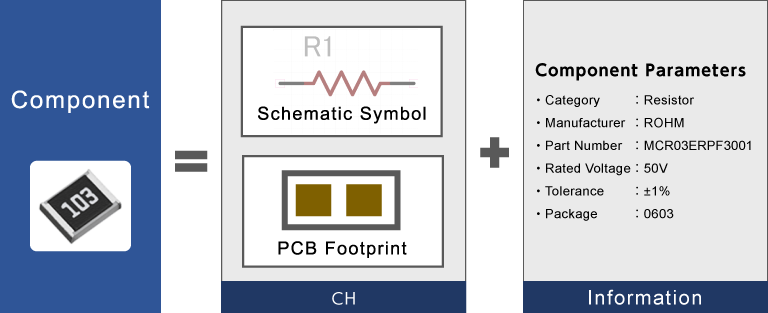
A Quadcept component is simply composed of two elements: models (symbol + footprint) and parametric component data.
Component Creation Sheet
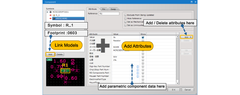
Let’s take a look at the Quadcept component creation sheet. Each model can be linked to the component in the Symbols region at the left side. For component parameters, you can add them in the Attribute tab. The image below shows how a ROHM’s component, MCR03ERPF3001 is created.
Naming Components, Symbols and Footprints
Component Name : MCR03ERPF3001, Symbol Name(Schematic) : R_1, Footprint Name (PCB) : 0603
Component Name
A manufacturer part number is often used for a component name in consideration of part procurement. For passive components such as resistors and capacitors, the symbol and footprint often have the same name.
Symbol Name
Generally, the schematic symbols for passive components such as resistors and capacitors are the same. For the component in the example, its symbol is the same among multiple manufacturers such as Rohm, Panasonic and Murata. Therefore, the symbol of the example is named “R-1” so that it can be shared among multiple components. (It is also good to name it “RES” or “R”.)
However, for components such as ICs, their symbols may have the same shapes but different pin layouts or electrical properties. So the manufacturer part numbers are often used for their names.
Footprint Name
For PCB footprints, designers often name them with a word that allows them to imagine footprint shapes such as 1608, 2125 and QFP64. For components such as ICs, their footprints could have different pad shapes or metal masks, so some information such as pad names or a gap between pads are sometimes added to the end of the footprint name.
What Parameters Are Required for a Component?
Required parametric component data differ depending on component categories.
In Quadcept, you are able to find and add suitable component parameters easily through direct connection to the web services provided by Digi-Key, Mouser Electronics, Chip1Stop, RS Components and CoreStaff.
Component parameters can be freely added to your components, but if you add a lot it will take more time to define them when you create a new component. It is important to determine what attributes you add in consideration of the balance between the benefits and costs of adding component parameters.
- Manufacturer Name
- Manufacturer Part Number
- Rated Power
- Rated Voltage
- Tolerance
- Package
- Operating Temperature
- Part Number for Digi-Key / Mouser Electronics / Chip1Stop / RS Components / CoreStaff
- Environmental Classifications
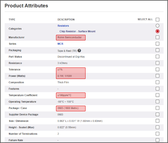
The following image shows the component data Digi-Key provides for a certain chip resistor. It contains a manufacturer name, tolerance, rated power, operating temperature and package out of the parameters listed above.
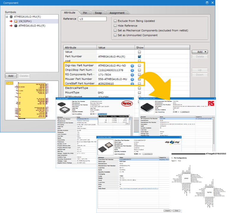
It is useful to register each part number of Digi-Key, Mouser Electronics, Chip1Stop, RS Components and CoreStaff to your components. It enables you to look up datasheets immediately whenever you want during design. More information such as stock information and prices from the distributors are also referable at any time. Those information helps you to select components, and even more, you can procure your required components more easily because BOM files can be generated in each supplier format. It also makes it easier to request part procurement to our online PCB design / manufacturing /assembly service, Elefab™.
The following image is the Component dialog. Adding each supplier’s part number and clicking the blue information icon next to it enables you to see the latest component data during design.
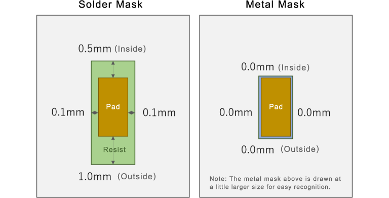
PCB Pad Layout Recommendations
Pads are basically created / placed according to datasheets offered by each manufacturer, but the size of the metal mask and solder mask sometimes is not described in the datasheets. This section introduces pad layout recommendations.
What Are Solder Mask & Metal Mask?
This section explains what solder mask and metal mask are.
Solder Mask
Solder mask, also known as a solder resist is a protective ink that is applied to the surface of a printed circuit board to prevent solder from adhering to unnecessary parts and causing a short circuit during mounting and to protect the copper from contaminants like dust and dirt.
Metal Mask
Metal mask is a solder paste stencil that is used to deposit the proper amount of solder paste onto the surface mount pads to establish electrical connections. Solder paste is needed to automatically place surface-mount devices onto a printed circuit board with robotic machines, commonly called pick-and-place machines.
Pad Layout Examples
The size of both masks will depend on your product, but for components such as ICs (SOP/QFP), the size of solder mask is generally larger than the copper pad. For metal mask its size is usually created the same size as the pad. (The following images show commonly defined pad size for solder and metal masks. For actually required size please make sure to check with PCB manufacturers or your customer.)
Making It Easier to Procure Components by Linking with Elefab™️
Part procurement is as tedious as part creation. One of Quadcept’s online web services, Elefab™️ makes it easier to get an estimate and place an order for PCB design, manufacturing, part procurement and assembly.
Linking with Elefab™ Services
The instructions that follow explain how you can connect to Elefab™ services from Quadcept.
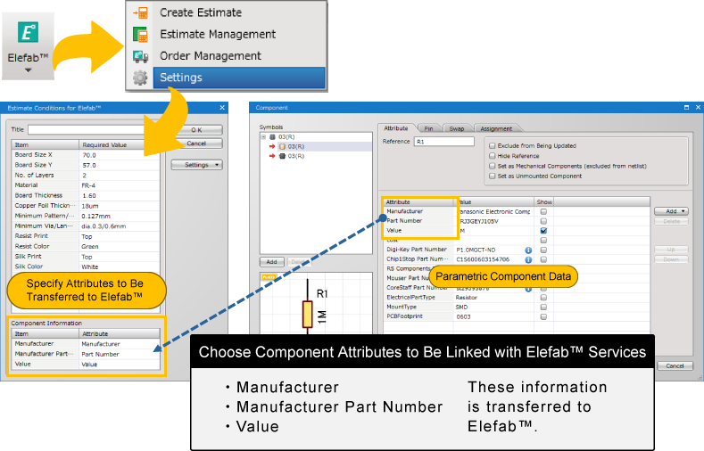
Go to the Completion tab in the ribbon menu and select [Elefab™] >> [Settings] to open the Estimate Conditions for Elefab™ dialog. In this dialog, specify the component properties to be transferred to the Elefab™ services in the Component Information region at the bottom of the dialog.

Just clicking on the Create Estimate button allows you to transfer your design information and estimate the pricing of your PCB manufacturing.
You do not have to attach the BOM file for your design.
By transferring your design information to the Elefab™ services directly from Quadcept, the components used in your design will be automatically extracted and displayed as a list. This allows you to instantly get an estimate or place an order without having to search for the parts or upload the BOM file.