This topic explains the basics of the Start Page and design screen in Quadcept.
Start Page
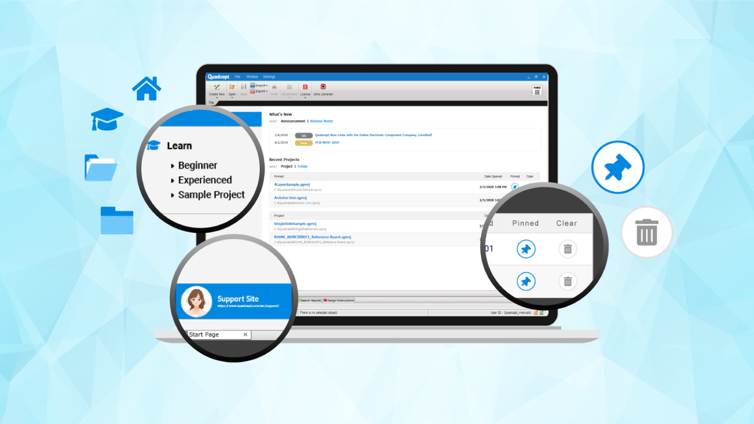
After you start up the Quadcept app, the Start Page below will be displayed on your screen. Every design will start from this page.
Recent Projects
Project files you have recently opened are shown as a list here. Your frequently used projects can be pinned to the Recent Projects for quick reference.
Learn
Sample projects are available here to help you learn the basics of Quadcept. This section also provides tutorials for Quadcept beginners to learn the basics, and advanced tips for experienced users to improve their skills.
New Project
Every design in Quadcept starts with a project file. You can create a new Quadcept project file from here.
Open Project
Clicking the Open Project icon allows you to open an existing project(*.qproj) onto the Project window.
Support Site
You can access our FAQ page, support forum, online manual and tutorial videos from here.
Moving Around the Design
The following methods can be used to pan around the design.
Panning Around the Design

You can pan around the layout by dragging while holding down the right mouse button.
Zooming In / Out
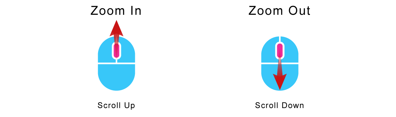
To zoom in or out the layout, you just scroll the mouse wheel.
Zooming in to a Specified Area (Marquee Zoom)

You can zoom in a particular area of your design, by dragging around that area while holding down the right and left mouse buttons. When you left-click while holding down just the right mouse button, the design will be zoomed out.
Your design can also be zoomed in / out with the keyboard.
| Zoom In | PageUP |
| Zoom Out | PageDown |
| Fit to Whole Design | 1 |
Design Screen
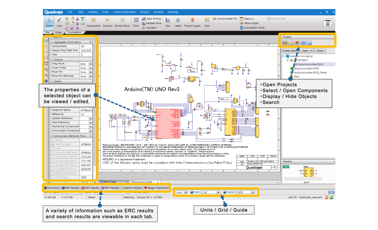
Circuit Designer
The sub windows located at the right side of the screen are frequently used during design.
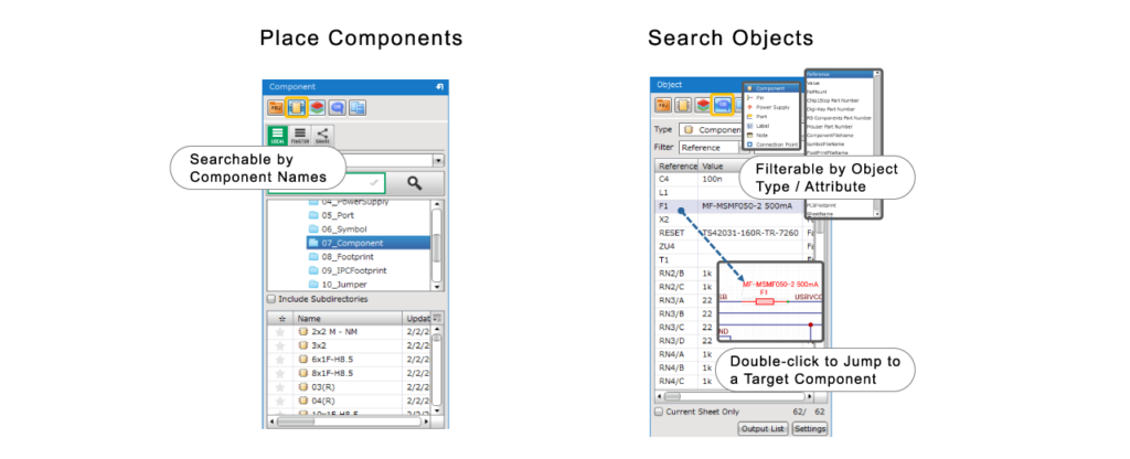
The Project window allows you to create a new project to start your design, or open an existing project to edit the layout. The Object window enables you to view the list of all the objects used in your project. With this window you are able to quickly find specific objects such as symbols and footprints placed on your design.
PCB Designer
The main screen of PCB Designer is basically the same as that of Circuit Designer. As frequently used features, this section explains the grid and layer settings.
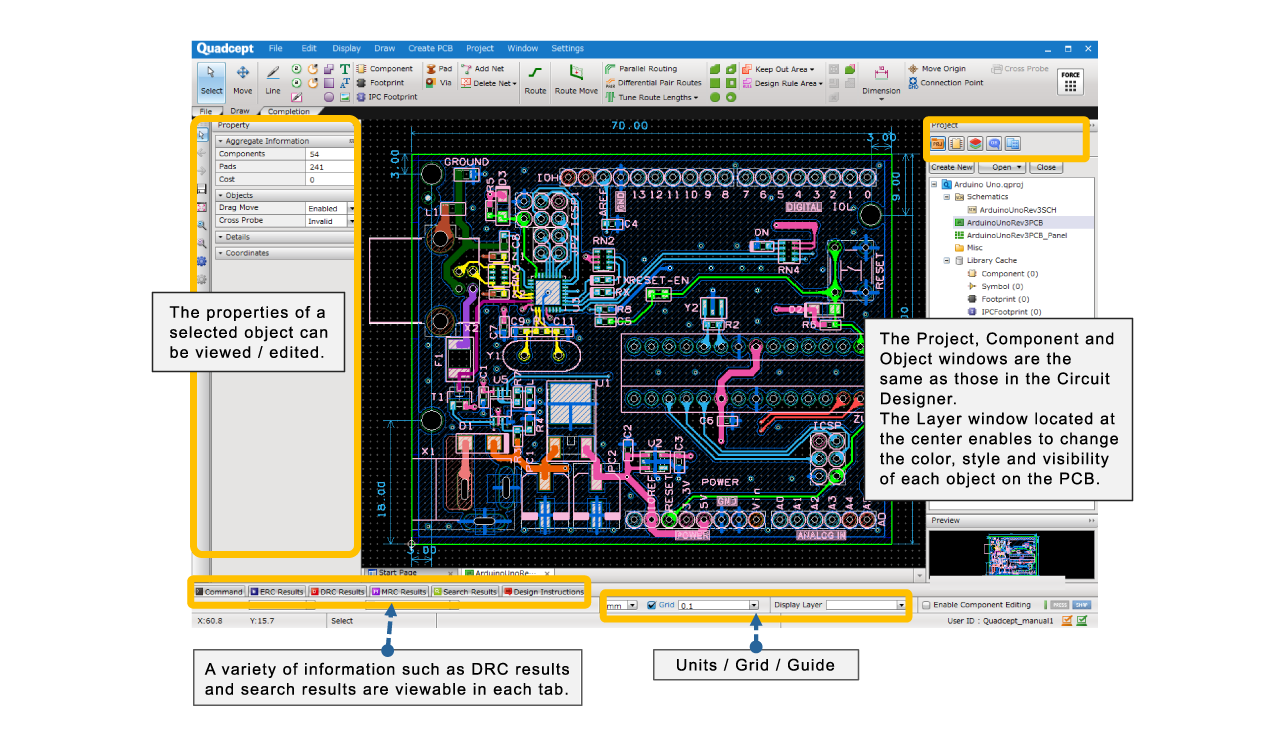
Configuring the Grid and Layer Settings
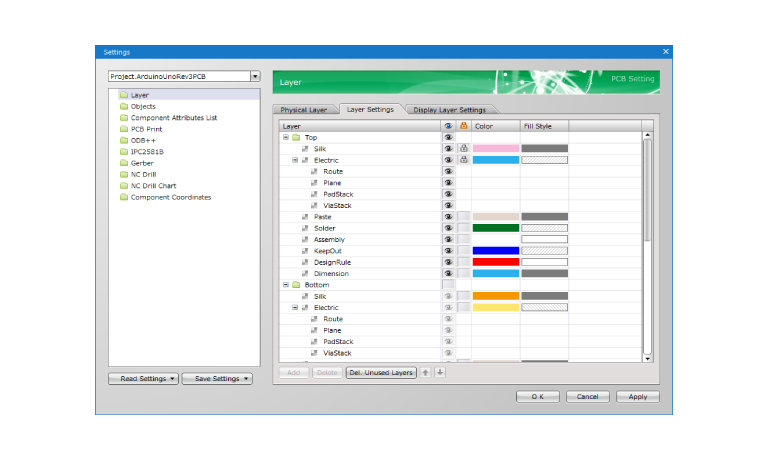
Since the step size for the grid and the display for the layers are frequently modified during design, they can be quickly changed within the design screen. You can also configure each setting in the Settings dialog that can be opened by selecting [Settings] >> [Settings]. If you work with multiple designers, it is important to share the default settings.
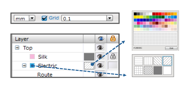
Grid Settings
It is recommended that the snap grid is changed according to design requirements such as design density and pattern width.
Layer Settings
- Show/Hide Clicking the eye icon allows you to toggle the visibility of a layer. You can easily toggle the state of multiple layers by dragging while holding down the left mouse button.
- Fill Style Click the fill style icon to change the fill style for objects placed on the layer. This is useful when you want to do a layout while displaying other layers.
- Color Click the color sample to change the fill color for objects placed on the layer.
- Lock If a lock mark is placed next to a layer, you will not be able to select / edit the objects on that layer. This is useful when you do not want to move objects such as board outlines.
Design Preparation
The sub windows explained above are useful for quickly changing the fill style or color for the objects during design, but if you start a new design you may want to configure the layer and grid settings beforehand.
The Settings dialog that can be opened by selecting [Settings] >> [Settings] allow you to configure various settings relating to schematic / PCB design. If you create your default settings here, then you will not have to configure them every time you start a new design.